Yesterday I fired off the Mk II PCB Gerber files into production and I should have the PCBs within a week.
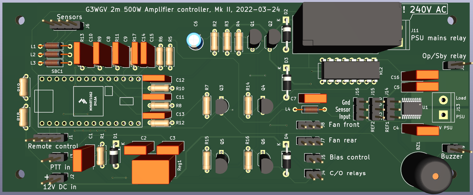 |
| The Mk II PCB in production, with INA253 current sensor |
One of the many things that delayed proceedings was concern about the introduction of surface mount devices (SMDs). I've never done anything with SMDs and my eyesight ain't as good as it was, so I was somewhat hesitant. In the end I decided that just as it is possible to teach old dogs new tricks so it should be possible to teach myself how to work with SMDs.
I bought an electronic microscope that projects a magnified image of the PCB onto my large PC screen and obtained a hot air gun, solder paste and tweezers. Importantly I also got an SMD practice board and I spent some time yesterday soldering teensy weensy capacitors, resistors and even ICs to it. The first attempts were rather pathetic but I quickly got the hang of how much solder paste to use (very little) and where to put it (at the end of the component solder pads). I think I am now good to go with soldering the INA253 current sensor, which is the only SMD on this PCB.
Coincidentally I have another PCB project on the go (a baud rate converter and radio modem for my weather station) and for that I have gone the whole hog on SMDs. It looks like a trend is developing here. I suspect, in time, that designing and building SMD boards will be as natural as the through-the-hole technology that I have been using for the last 50 years.
I shall report back in due course.